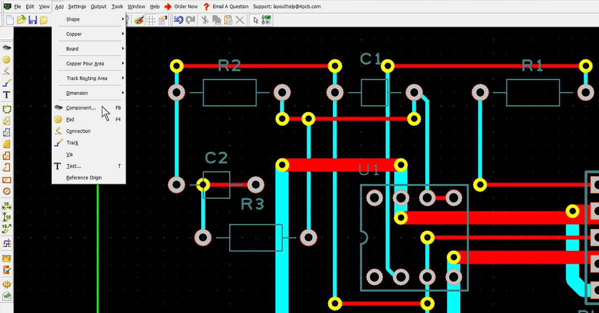
PCB layout:
The printed circuit board design process includes schematic design, electronic component database registration, design preparation, block segmentation, electronic component configuration, configuration verification, wiring and final inspection.
Printed cirucit board(PCB) layout services is one of the ways that we help our customers get to market faster as our engineers teams has significant practical experience in layout design performance.
Our capacity:
More than 10 years of experience in electronic design and software design. Cost-optimized design guides our experienced engineers when developing your products according to your expectations: from the specification sheet via approvals and validations up to the series production.
Full design flow from start to finish :
Micro BGA / Micro Via / Blind and Buried Vias
Rules Driven Designs
Schematic Capture
Library Development
Database Construction and Verification
Signal Integrity/Design Verification
EMI Checking
Full Document Package Creation
Electrical Engineering
Our services:
Performing the physical pcb layout of your design
PCB manufacture
PCB Assembly(SMT+DIP)
Enclosure design&Open new mold
Housing assembly
Function test
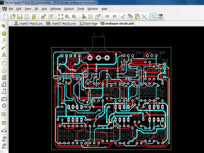
PCB layout cases: